SOME OF OUR AMAZING WORK
Scroll through for images of some of the awesome projects we have done in the past. With decades of work across multiple industries, we have had the chance to do a thing or two.

"We will be the leading provider of quality and innovative industrial repair and maintenance solutions for the indian Market while ensuring corporate integrity, employee safety, and customer satisfaction"
Scroll through for images of some of the awesome projects we have done in the past. With decades of work across multiple industries, we have had the chance to do a thing or two.
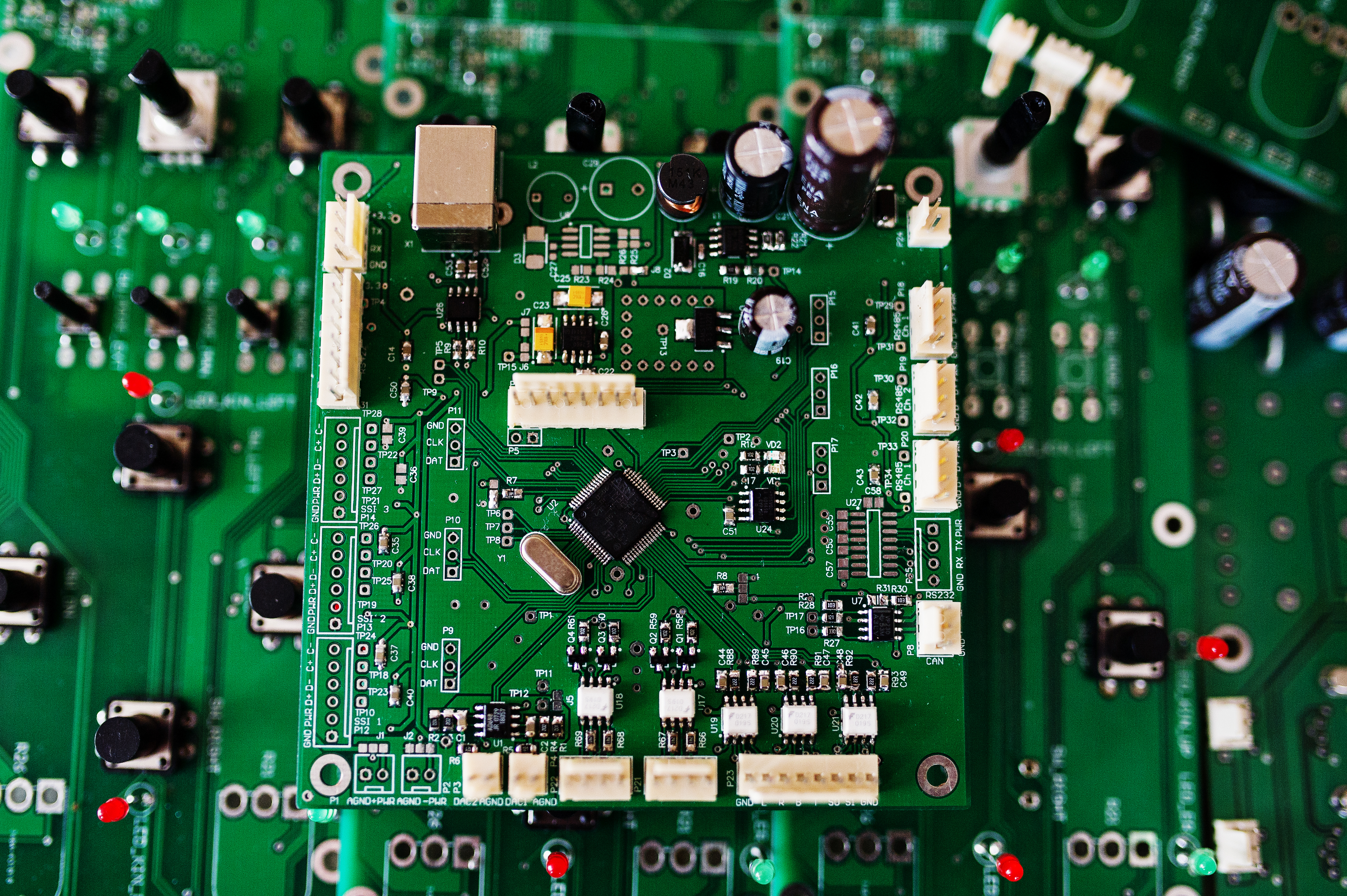
Harness the potential of your entire design and engineer teams to solve the most complex design challenges. Collaborate across the wall, across design domains, ona single design or a complex multi-board PCB system. Track your design projects to success as design rules and design goals are established and met.

Simulate early, simulate often

Simplify the complex

Build your teamwork
A complete, integrated, simulation-driven design solution for your entire electronic product design team.
Easy-to-use system architecture planning and schematic capture environment
Complete rules-based real-time PCB layout and routing environment
Manage a shared library of parts, symbols and footprints to reduce time and errors
Accurate modeling, design optimization, and validation to ensure functionality
Advanced integrated PI power-aware SI tools to ensure better design performence
Signal and power integrity analysis with sign-off level accuracy
Accurate Services
Field Service Hour
Satisfied Customer
Satisfied employee
Our team is on standby to help you with your industrial manufacturing, maintenance and repair needs as well as your process, safety and flow control needs. Contact us today, and we'lll get started.
| SPECIFICATION | STANDARDS |
|---|---|
| Minimum conductor width | 6 mils |
| Minimum conductor spacing/air gap | 6 mils |
| Minimum Plated hole size | 16 mils |
| Maximum Plated hole size | 240 mils |
| Maximum board size | 300 mm * 350 mm |
| Maximum number of layers | 2 |
| Minimum copper thickness | 1 Oz(35 micron) |
| Maximum copper thickness | 3 Oz(105 micron) |
| Dedicated Electrical Testing | Available |
| PCB Cutting option | Routing, V groove, Punching |